Surface Mount Devices (SMDs) are electronic components mounted directly onto the surface of a printed circuit board (PCB). Their small size has become integral to the efficiency of electronic devices.
Let’s start by exploring the benefits of SMDs, as opposed to traditional through-holes:
| Benefit | Description |
| :=== | :=== |
| Miniaturization | SMDs enable electronic miniaturization, crucial for space-constrained applications. |
| High-Density Assembly | SMDs allow for high-density PCB assembly, optimizing component placement for increased overall density. |
| Improved Electrical Performance | Shorter lead lengths in SMDs reduce parasitic elements, enhancing high-frequency performance and signal integrity. |
| Reduced Signal Interference | Compact size and direct PCB placement minimize loop areas, reducing electromagnetic interference EMI. |
| Automated Manufacturing | SMDs are compatible with automated pick-and-place, ensuring efficient and precise mass production with cost savings. |
| Lower Weight and Cost | SMDs contribute to lighter devices, and automated assembly reduces manufacturing costs.|
| Enhanced Thermal Performance | SMDs with exposed metal pads improve thermal dissipation, enhancing overall thermal performance. |
| Better Mechanical Stability | SMDs, soldered directly to PCBs, provide superior mechanical stability, making them more resistant to shocks, vibrations, and mechanical stresses. |
SMD Packaging for Passive Components
Surface Mount Device (SMD) packaging for passive components, such as resistors, capacitors, and inductors, involves a variety of package types:
Chip Resistors and Capacitors (Standard Ceramic Packages)
Packages: The most common SMD package for chip resistors and capacitors is the ceramic chip package. It comes in various standardized sizes, such as 0402, 0603, 0805, and 1206.
Materials: Typically made of ceramic materials with conductive layers for electrodes and dielectric layers for capacitors.
Advantages: Compact size, suitable for high-density applications.
Tantalum Capacitors
Packages: Tantalum capacitors come in SMD packages like the molded tantalum chip (MTC) and molded tantalum leadframe (MTL) packages.
Materials: Tantalum-based dielectric material with a metal case for encapsulation.
Advantages: Higher capacitance values in a compact size, suitable for applications requiring stable capacitance over a wide temperature range.
Aluminum Electrolytic Capacitors
Packages: SMD aluminum electrolytic capacitors are available in various configurations, including cylindrical and chip-type packages.
Materials: Aluminum-based electrolyte with a metallic case.
Advantages: Larger capacitance values compared to ceramic capacitors, suitable for applications requiring higher energy storage.
Multilayer Ceramic Capacitors (MLCC)
Packages: MLCCs are available in various standard sizes, including 0402, 0603, 0805, 1206, and larger.
Materials: Multilayered ceramic structure with alternating layers of ceramic and conductive material.
Advantages: High capacitance density, suitable for high-frequency applications and decoupling.
SMD Packaging for Active Components
| Category | Package | Types | Materials | Advantages |
| :=== | :=== | :=== | :=== | :=== |
| Transistors | SOT (Small Outline Transistor) | SOT-23, SOT-89, SOT-223 | Plastic or epoxy resin with metal leads | Compact size, suitable for low to medium-power discrete transistors |
| Integrated Circuits (ICs) | QFN (Quad Flat No-Lead) | Compact, leadless with exposed thermal pad on the bottom | Plastic or ceramic with metal leads/pads | Compact, suitable for high-density integration, various pin counts, and configurations |
| | TQFP (Thin Quad Flat Package) | Flat, square-shaped with gull-wing leads | | |
| | SOIC (Small Outline Integrated Circuit) | Small, rectangular with gull-wing leads | | |
| | SSOP (Shrink Small Outline Package) | Similar to SOIC but with a smaller body size | | |
| Microcontrollers | LQFP (Low-profile Quad Flat Package) | Common sizes: 32, 48, 64, 100 pins | Plastic or ceramic with gull-wing leads | Good balance between size and ease of soldering, suitable for microcontroller applications |
| Ball Grid Array (BGA) | BGA (Ball Grid Array) | PBGA (Plastic BGA), CBGA (Ceramic BGA) | Plastic or ceramic with solder balls | High pin count, compact design, excellent thermal performance, suitable for high-performance applications |
| Chip-on-Board (COB) | COB (Chip-on-Board) | Bare semiconductor chips mounted on PCB, wire bonding | Semiconductor chips and wire bonds | Compact, cost-effective for high-volume applications, flexibility in design |
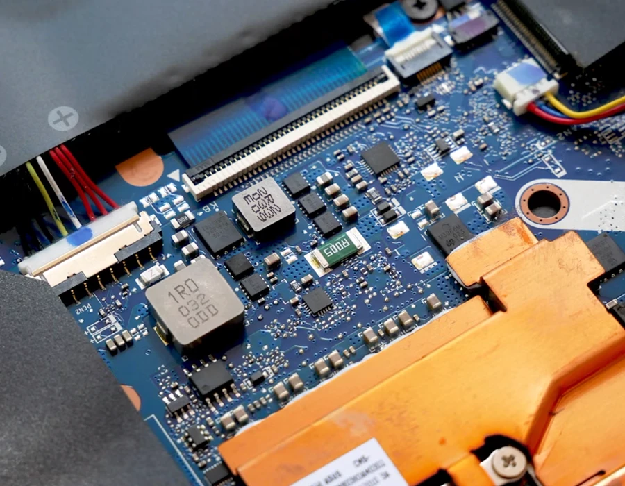
Motherboard utilizing surface mount technology
Challenges with Surface Mount Devices
SMDs come with their own set of challenges during assembly and use:
Tombstoning: Tombstoning occurs when one end of a passive SMD component is vertically displaced during reflow soldering, resembling a tombstone. This anomaly may arise from uneven heating profiles, inadequacies in solder paste deposition, or irregularities in component placement precision.
Solder Bridging: Solder bridging involves unintended connections between adjacent pads, leading to short circuits. Root causes include excessive solder paste application, suboptimal stencil design, or inadequate implementation of solder mask features.
Skew and Misalignment: Skew and misalignment issues materialize when SMD components deviate from precise placement on PCB pads during the pick-and-place process. These discrepancies can result in compromised solder joints and consequential performance degradation.
Insufficient Solder Joints: Incomplete or inadequate solder joints may occur due to factors such as insufficient solder paste deposition, suboptimal reflow soldering conditions, or inaccuracies in component placement. These deficient joints can yield intermittent electrical connections or outright failures.
Let’s start by exploring the benefits of SMDs, as opposed to traditional through-holes:
| Benefit | Description |
| :=== | :=== |
| Miniaturization | SMDs enable electronic miniaturization, crucial for space-constrained applications. |
| High-Density Assembly | SMDs allow for high-density PCB assembly, optimizing component placement for increased overall density. |
| Improved Electrical Performance | Shorter lead lengths in SMDs reduce parasitic elements, enhancing high-frequency performance and signal integrity. |
| Reduced Signal Interference | Compact size and direct PCB placement minimize loop areas, reducing electromagnetic interference EMI. |
| Automated Manufacturing | SMDs are compatible with automated pick-and-place, ensuring efficient and precise mass production with cost savings. |
| Lower Weight and Cost | SMDs contribute to lighter devices, and automated assembly reduces manufacturing costs.|
| Enhanced Thermal Performance | SMDs with exposed metal pads improve thermal dissipation, enhancing overall thermal performance. |
| Better Mechanical Stability | SMDs, soldered directly to PCBs, provide superior mechanical stability, making them more resistant to shocks, vibrations, and mechanical stresses. |
SMD Packaging for Passive Components
Surface Mount Device (SMD) packaging for passive components, such as resistors, capacitors, and inductors, involves a variety of package types:
Chip Resistors and Capacitors (Standard Ceramic Packages)
Packages: The most common SMD package for chip resistors and capacitors is the ceramic chip package. It comes in various standardized sizes, such as 0402, 0603, 0805, and 1206.
Materials: Typically made of ceramic materials with conductive layers for electrodes and dielectric layers for capacitors.
Advantages: Compact size, suitable for high-density applications.
Tantalum Capacitors
Packages: Tantalum capacitors come in SMD packages like the molded tantalum chip (MTC) and molded tantalum leadframe (MTL) packages.
Materials: Tantalum-based dielectric material with a metal case for encapsulation.
Advantages: Higher capacitance values in a compact size, suitable for applications requiring stable capacitance over a wide temperature range.
Aluminum Electrolytic Capacitors
Packages: SMD aluminum electrolytic capacitors are available in various configurations, including cylindrical and chip-type packages.
Materials: Aluminum-based electrolyte with a metallic case.
Advantages: Larger capacitance values compared to ceramic capacitors, suitable for applications requiring higher energy storage.
Multilayer Ceramic Capacitors (MLCC)
Packages: MLCCs are available in various standard sizes, including 0402, 0603, 0805, 1206, and larger.
Materials: Multilayered ceramic structure with alternating layers of ceramic and conductive material.
Advantages: High capacitance density, suitable for high-frequency applications and decoupling.
SMD Packaging for Active Components
| Category | Package | Types | Materials | Advantages |
| :=== | :=== | :=== | :=== | :=== |
| Transistors | SOT (Small Outline Transistor) | SOT-23, SOT-89, SOT-223 | Plastic or epoxy resin with metal leads | Compact size, suitable for low to medium-power discrete transistors |
| Integrated Circuits (ICs) | QFN (Quad Flat No-Lead) | Compact, leadless with exposed thermal pad on the bottom | Plastic or ceramic with metal leads/pads | Compact, suitable for high-density integration, various pin counts, and configurations |
| | TQFP (Thin Quad Flat Package) | Flat, square-shaped with gull-wing leads | | |
| | SOIC (Small Outline Integrated Circuit) | Small, rectangular with gull-wing leads | | |
| | SSOP (Shrink Small Outline Package) | Similar to SOIC but with a smaller body size | | |
| Microcontrollers | LQFP (Low-profile Quad Flat Package) | Common sizes: 32, 48, 64, 100 pins | Plastic or ceramic with gull-wing leads | Good balance between size and ease of soldering, suitable for microcontroller applications |
| Ball Grid Array (BGA) | BGA (Ball Grid Array) | PBGA (Plastic BGA), CBGA (Ceramic BGA) | Plastic or ceramic with solder balls | High pin count, compact design, excellent thermal performance, suitable for high-performance applications |
| Chip-on-Board (COB) | COB (Chip-on-Board) | Bare semiconductor chips mounted on PCB, wire bonding | Semiconductor chips and wire bonds | Compact, cost-effective for high-volume applications, flexibility in design |
Motherboard utilizing surface mount technology
Challenges with Surface Mount Devices
SMDs come with their own set of challenges during assembly and use:
Tombstoning: Tombstoning occurs when one end of a passive SMD component is vertically displaced during reflow soldering, resembling a tombstone. This anomaly may arise from uneven heating profiles, inadequacies in solder paste deposition, or irregularities in component placement precision.
Solder Bridging: Solder bridging involves unintended connections between adjacent pads, leading to short circuits. Root causes include excessive solder paste application, suboptimal stencil design, or inadequate implementation of solder mask features.
Skew and Misalignment: Skew and misalignment issues materialize when SMD components deviate from precise placement on PCB pads during the pick-and-place process. These discrepancies can result in compromised solder joints and consequential performance degradation.
Insufficient Solder Joints: Incomplete or inadequate solder joints may occur due to factors such as insufficient solder paste deposition, suboptimal reflow soldering conditions, or inaccuracies in component placement. These deficient joints can yield intermittent electrical connections or outright failures.
Share
Jharwin Barrozo
Jharwin is an electronics engineer mainly focused on satellites. He built his own ground station using Flux to monitor RF activities on the International Space Station. Find him on Flux @jharwinbarrozo
Go 10x faster from idea to PCB
Work with Flux like an engineering intern—automating the grunt work, learning your standards, explaining its decisions, and checking in for feedback at key moments.
This comprehensive guide explores the roles and types of electrical connectors in any wiring project. From crimping tools to wire strippers, it outlines the tools and techniques needed for efficient electrical wiring. The post also provides safety tips and insights into specialized connectors.
If you're a lover of smart home devices, you're likely buzzing with excitement over Arduino's recent collaboration with Silicon Labs. We are too, and we’re even more excited to bring the power of this collaboration to life on Flux. As of today, we’re excited to announce that engineers can fully design Arduino-based Matter boards with Flux.
Circuit simulation is a crucial tool in electronic design. It uses software to predict how circuits will perform, saving time and money. Popular options like Flux, LTSpice, and CircuitMaker offer powerful features.
A voltage drop calculator is an essential tool for assessing the decrease in voltage across a conductor, ensuring electrical devices receive adequate power for optimal operation. Read our blog to learn more.
Explore the essentials of schematic diagrams in our comprehensive guide, covering everything from basic resistors to complex integrated circuits, and learn to master the visual language of electronics.
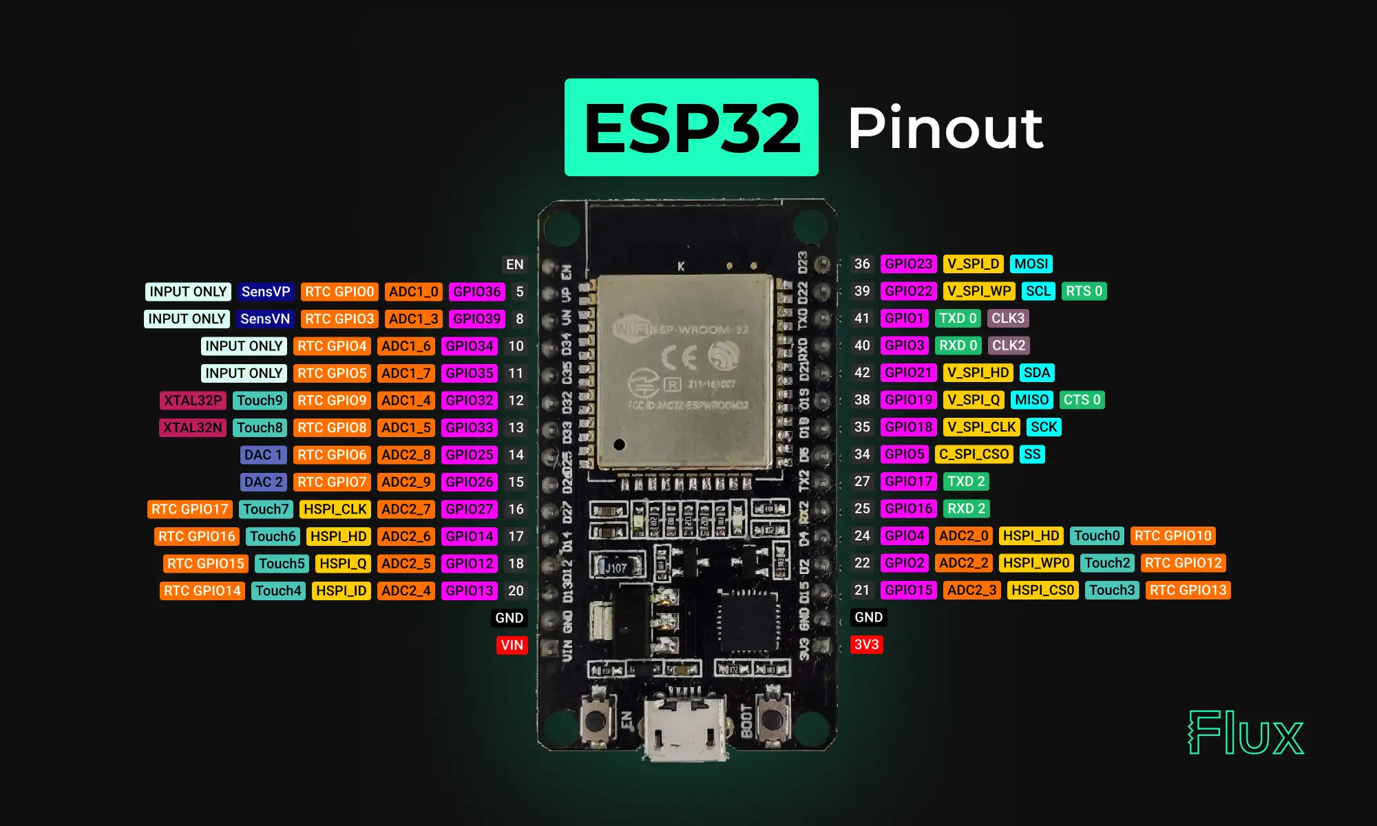
Looking for a comprehensive guide to ESP32 pinout? Check out our article that covers everything you need to know about the ESP32's pins, including digital, analog, PWM, and Strapping pins. Perfect for beginners and experts alike, our guide will help you understand the ESP32's pinout and how to use it in your projects.
Before you start this exciting journey, it's essential to equip yourself with the right knowledge, tools, and preparations. This article offers practical insights and suggestions to help you lay a strong foundation for your PCB design projects.
In this post, we’ll explore why these concepts matter, how they impact signal integrity and power distribution, and what to keep in mind as you design. If you want to go deeper into implementation details—like when to use zones, where to place stitching vias, or how to avoid stack-up pitfalls—we’ve created a detailed PDF guide just for that.
This blog post highlights a series of innovative reference designs developed by renowned manufacturers using Flux. These reference designs encompass a variety of applications, including advanced light sensing, robust data communication, and compact distance measurement. This diverse array showcases the adaptability and effectiveness of Flux in meeting the varied needs of industrial sensing applications
Managing inductive loads in electronics can pose challenges due to voltage spikes. The flyback diode serves as a protective component, preventing damage to delicate parts like transistors. This article dives deep into its functionality, types, and real-world applications.
The blog is an educational resource on netlists, detailing their role as intermediaries between circuit schematics and physical layouts. Special attention is given to different types of netlists, such as FPGA and RTL. It outlines the crucial role of accurate netlists in hardware functionality and discusses the various formats used in the design process.
Easily calculate resistor values with Flux online Resistor Color Code Calculator. This powerful tool saves time and eliminates errors for electronics enthusiasts and professionals.